You spend thousands of hours and millions of dollars designing a flawless silicon architecture, but if the physical housing fails, the entire component is worthless. The barrier between a functioning electronic brain and a piece of scrapped silicon is the encapsulation. This comprehensive guide breaks down the complex world of modern electronic packaging. It is worth reading because understanding the specific materials, thermal dynamics, and mechanical stresses involved in protecting silicon will drastically improve your production yields. Whether you are managing a high-volume assembly line or sourcing precision tools to machine the molds themselves, mastering these fundamental concepts will save you time, reduce costly scrap, and give you a massive competitive edge in the market.
What is an ic package and why does encapsulation matter in the semiconductor industry?
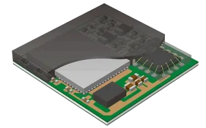
At its core, an ic package is the protective armor that surrounds a fragile piece of silicon. Without this vital protective layer, the bare chip would instantly succumb to environmental hazards like moisture, dust, and physical impact. The primary goal of encapsulation is to completely seal the delicate internal structures from the outside world. This guarantees that the component will function reliably for years, whether it is installed in a climate-controlled server room or under the hood of a vibrating automobile.
In the global semiconductor industry, the physical housing also serves as a critical bridge. It transforms the microscopic connection points on the silicon into a larger, standardized footprint that can actually be soldered onto a pcb (printed circuit board). This means the chosen package type directly dictates how the component integrates into the final product. A poorly chosen housing can lead to overheating, signal degradation, or mechanical failure during standard operation.
The manufacturing technology behind this process is staggering. We are taking something as fragile as an eggshell and encasing it in rock-hard synthetic materials. Today, the most common components you see on a board are surface mount devices. Whether dealing with a simple smd component or a complex multi-core processor, the exact same principle applies: the outer shell must be absolutely perfect.
How do packaging processes protect the delicate chip from damage?
The journey from a bare piece of silicon to a finished, mountable product is highly complex. The modern manufacturing process employs a variety of sophisticated techniques to ensure absolute reliability. One of the most critical packaging processes involves establishing the electrical connections before the final sealing occurs. For instance, in advanced flip-chip assembly, the active area of the silicon is flipped upside down. It connects directly to the underlying structure using tiny metal bumps.
This specific flip chip approach drastically reduces the distance the electrical signal must travel. It provides excellent electrical performance. However, these microscopic solder bumps require immense protection. Once the interconnection is successfully made, the entire assembly must be locked securely in place. The protective material flows around these tiny joints, providing rigid mechanical support and preventing them from cracking under stress.
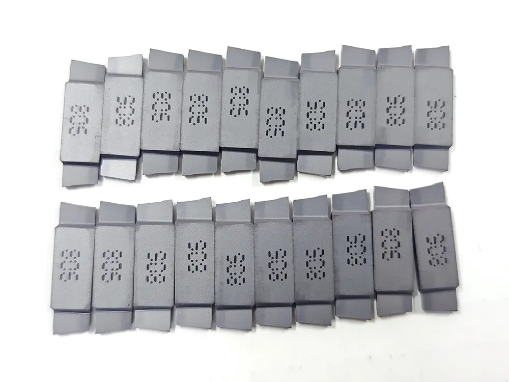
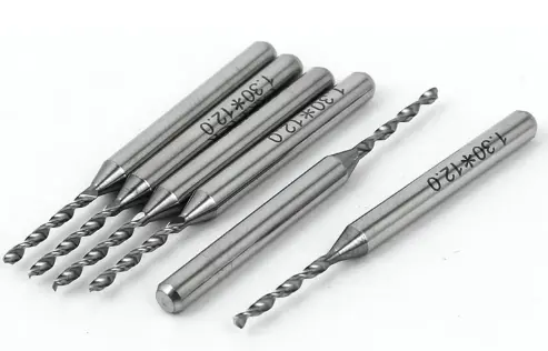
Achieving this level of precision requires incredibly accurate physical tooling. The metal molds used to shape the final protective shell must be machined to exacting tolerances. When fabricating these heavy steel molds, toolmakers rely on high-performanceCarbide Drills to cleanly cut cooling channels and injector ports without leaving burrs that could disrupt the fluid flow of the protective plastics.
What is epoxy mold compound and why is it widely used?
When we talk about the black plastic body of a standard microchip, we are almost always talking about an epoxy mold. This material is a specialized thermoset plastic. Unlike everyday plastics that can be melted and reshaped, a thermoset undergoes an irreversible chemical reaction when heated. Once it cures, it forms an incredibly hard, durable, and permanent shell.
An epoxy mold compound (commonly referred to as emc) is essentially a heavily engineered chemical cocktail. It consists of a base epoxy resin, hardening agents, and massive amounts of silica filler. The silica is crucial because it significantly lowers the material’s expansion rate when exposed to heat. These emcs represent the absolute backbone of modern plastic component housing. The materials used must also possess excellent dielectric properties, ensuring they act as perfect electrical insulators to prevent internal short circuits.
“The consistency of your molding material directly dictates the consistency of your final product. In high-stakes manufacturing, predictability is profitability.”
How does the molding compound interface with the substrate and interconnect?
During the actual injection phase, the hot, viscous molding compound is forced into a steel cavity under immense pressure. It must flow smoothly over the delicate silicon and the underlying substrate. This is a violent process. If the fluid dynamics are not perfectly controlled, the rushing fluid can literally sweep away the tiny gold wires that form the interconnect.
Furthermore, the fluid must completely fill every single microscopic cavity within the mold. Any trapped air creates a void. A single void is considered a catastrophic defect. If moisture accumulates inside a void, the heat of a standard reflow soldering oven will turn that moisture into steam, literally blowing the component apart from the inside (known as the “popcorn effect”).
To prevent this, the interface between the protective plastic and the metal lead frame must be chemically robust. Proper substrate design plays a huge role here. Engineers often design interlocking physical features or apply specialized chemical adhesion promoters to ensure the plastic grips the metal flawlessly.
What role does the wafer play before singulation?
Historically, silicon was diced into individual pieces before being packaged. However, to maximize efficiency and optimize the footprint, the industry developed wafer-level packaging. In this advanced methodology, the entire round silicon disc is processed and sealed simultaneously before any cutting takes place.
During this stage, a layer of protective material covers the entire top surface of the unbroken disc. Only after the protective layer has fully cured does the process of singulation begin. Singulation is the brutal mechanical process of slicing the large, sealed disc into thousands of individual, final components.
This cutting process is notoriously difficult because the saw blade must cut through both the hard silicon and the abrasive silica-filled plastic simultaneously. It requires incredibly tough and stable cutting tools. Just as a machinist uses specialized Solid Tungsten Carbide Rods to endure abrasive wear on the CNC floor, the dicing blades must withstand extreme friction to prevent chipping the delicate edges of the newly formed components.
How are systems like LPKF driving laser processing and fabrication forward?
As the demand for extreme miniaturization grows, traditional mechanical cutting saws are reaching their absolute physical limits. When you are building components for smartwatches or medical implants, a mechanical blade is simply too thick and too rough. This is where advanced laser systems, like those pioneered by lpkf, step in to revolutionize the workflow.
Laser processing is now a fundamental part of modern fabrication. Instead of grinding through the material, high-powered lasers instantly vaporize the epoxy mold compound and the silicon beneath it. This clean ablation process leaves incredibly smooth edges and allows for much tighter spacing between components on the production line.
This massive advancement means that structures can be cut and shaped with a precision of just a few µm (micrometers). By combining advanced laser ablation with traditional lithography, manufacturers can create highly complex, three-dimensional package shapes that were physically impossible to produce just a decade ago.
Why are vias and advanced routing crucial for high-density ICs?
Modern processors are not just single flat squares; they are complex, multi-layered skyscrapers of data. As we pack more functions into a single space, the routing of the electrical signals becomes a monumental geometric challenge. The internal pathways must be incredibly short to maintain speed and reduce power consumption.
To achieve this, engineers utilize tiny, vertically drilled holes called vias. These microscopic tunnels are plated with a conductive metal, usually cu (copper), to connect the different layers of the substrate or the internal redistribution layer. The rdl is essentially a microscopic highway system that reroutes the ultra-fine connections on the silicon die to the larger solder balls on the exterior.
This high-density layout is an absolute necessity for modern computing. Sometimes, traditional subtractive etching cannot achieve the necessary fine lines. In these cases, additive manufacturing techniques are utilized to slowly build up the exact copper traces required.
- Higher Pin Counts: More complex chips require more connections.
- Shorter Signal Paths: Vertical connections drastically reduce signal delay.
- Reduced Footprint: Layering allows for smaller overall device sizes.
What are the challenges with thermal expansion and warpage during molding?
Heat is the ultimate enemy of precision manufacturing. During the high-temperature curing phase, all materials expand. The severe problem arises because there is a massive mismatch in the thermal expansion rates between the pure silicon die, the copper lead frame, and the plastic shell.
We measure this expansion using the coefficient of thermal expansion (or cte). If the CTE is not carefully balanced, the entire assembly will warp as it cools down to room temperature. It literally bows like a potato chip. This warpage is a nightmare for board assembly. If the component is not perfectly flat, the solder joint will fail during the smt (surface mount technology) attachment process.
To combat this, engineers utilize sophisticated design tool software to simulate the thermal stresses before a physical prototype is ever built. They carefully adjust the silica filler content in the epoxy mold to ensure its CTE closely matches that of the underlying board. It is a delicate balancing act of chemistry and physics.
Standard packaging techniques are completely inadequate for the extreme demands of 5g communication and advanced radar systems. At these ultra-high frequencies, the physical housing itself can severely interfere with the radio signals. We must relentlessly pursue improved performance by utilizing specialized materials.
For a high-frequency sensor or antenna, the electrical properties of the molding compound are scrutinized heavily. If the material absorbs too much electromagnetic energy, the signal dies. Therefore, specialized low-loss resins are formulated specifically to let these high-speed signals pass through without degradation.
Furthermore, we see the rise of the advanced ic architecture. Concepts like heterogenous integration and package-on-package allow different specialized components—like memory and processing logic—to be stacked vertically. This keeps the signal paths incredibly short, drastically enhancing the overall electrical and thermal performance. When precision matters, utilizing high-quality tooling like aTriple-Blade (3-Flute) End Mill ensures the test fixtures holding these high-speed devices are perfectly flat and true.
Can a solid polymer thermoset really prevent corrosion and defects?
Absolutely. The primary defense against the harsh realities of the physical world is the integrity of the polymer shell. Whether it is a simple discrete power transistor or a highly complex quad flat no-lead (qfn) microcontroller, the ultimate goal is zero moisture ingress. Water vapor is the leading cause of internal corrosion and premature failure in deployed electronics.
To achieve this perfect seal in high-volume production, manufacturers choose different methods based on the strict application requirements. Liquid molding might be used for incredibly delicate, thin assemblies where low injection pressure is mandatory to prevent wire sweep. Conversely, solid compression molding is often preferred for large, flat panels because it provides excellent uniformity and high throughput.
Every single step in the design and manufacturing phase requires a strict methodology. There is always a tradeoff between cost, speed, and absolute reliability. However, by demanding strict material controls and utilizing innovative solutions, the industry continues to produce billions of flawless devices every year. The suitability of the materials used in ic fabrication ultimately determines the lifespan of the technology we rely on daily.
Summary of Key Takeaways:
- The ic package provides vital physical protection and essential electrical routing for the fragile silicon.
- Epoxy mold compound acts as the primary defense against moisture, shock, and internal corrosion.
- Advanced packaging processes require pristine interconnect integrity to ensure strong electrical properties.
- Managing the thermal expansion (cte) is critical to prevent warpage and ensure perfect smt board mounting.
- The pursuit of high-performance in 5g applications relies entirely on optimizing both the package design and the specific molding chemistry.
- Successful assembly and testing depends on precision tooling, strict fluid dynamic control, and advanced ic technology.
- From traditional flip chip designs to modern heterogenous stacking, the versatility of the package performance drives the entire tech industry forward.
- A semiconductor cannot function in the real world without a perfectly engineered, thermally stable plastic housing.