This comprehensive guide will dive deep into the specifics of making holes in advanced electronics boards. Whether you’re working on a simple prototype or complex multi-layer boards, understanding the minimum drill size and drill configurations is absolutely crucial for your success. It is worth reading because getting your drill parameters right will dramatically reduce costs, avoid common pitfalls, and ensure your PCB performs as intended. Learn key features of the drilling process that keep high-speed designs functional and manufacturable on the modern shop floor.
When you manage a production line or supply tools to a busy shop, predictability is everything. You cannot afford to have a drill snap mid-cycle. You need to know exactly how the drill interacts with the plate. In this guide, we will break down the mechanics of the pcb drill, explore the limitations of mechanical drilling technology, and explain how to optimize your circuit layouts.
What exactly is a PCB drill and why do drill sizes matter so much?
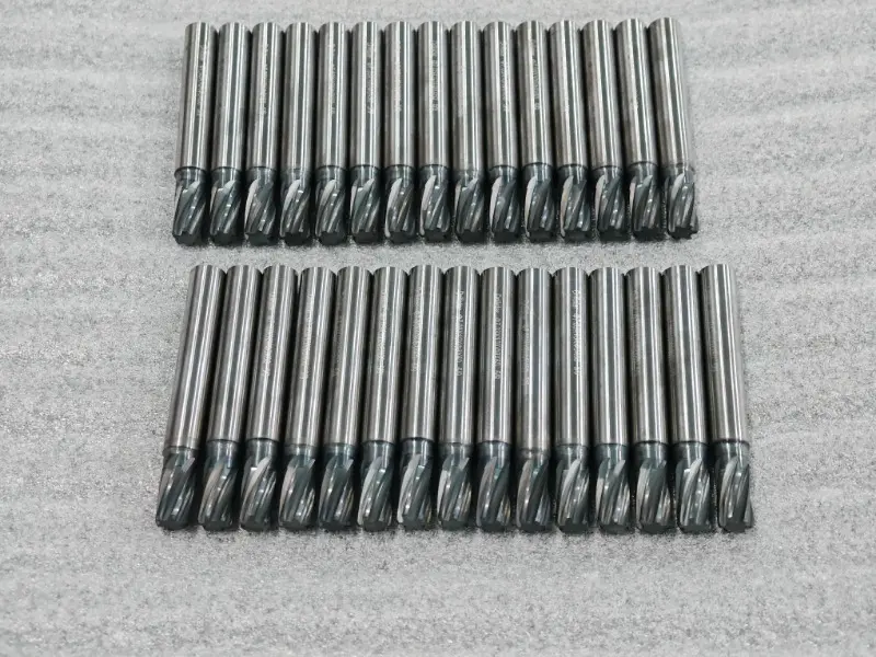
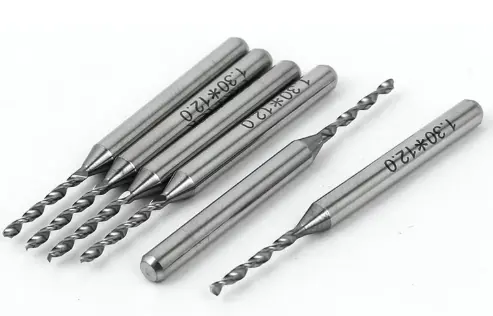
When you look closely at a printed circuit board, you see hundreds, sometimes thousands, of tiny holes. To create these holes efficiently, factories use a highly specific pcb drill. A standard pcb drill is a specialized cutting tool made entirely from solid carbide. You might wonder why we don’t use standard steel. The reason is simple. The fiberglass plate used to make a circuit is incredibly abrasive. It will dull a normal steel drill in seconds. A solid carbide drill stays sharp, cutting cleanly through the glass and copper layers.
Choosing the correct drill sizes is one of the most important aspects of pcb design. The drill size and drill requirements you select dictate exactly how well your through-hole components will fit later on the assembly line. If the drill creates a hole that is too tight, the assembly workers cannot insert the parts. If the drill creates a hole that is too loose, the solder will not hold the component lead securely.
If you pick incorrect drill sizes, you will quickly increase manufacturing costs. During pcb manufacturing, a CNC machine must physically swap out each drill bit for different hole sizes. By limiting the number of unique drill sizes in your design, you speed up the overall drilling process. Every time a new drill is loaded into the spindle, the chance for a mechanical error goes up. Therefore, picking optimal drill sizes ensures your circuit goes into mass production smoothly. You should always stick to standard drill sizes to keep your pcb fabrication budget as low as possible.
How do you determine the minimum drill size for your circuit?
Every pcb manufacturer operates under strict physical limits. The minimum drill size represents the absolute smallest mechanical drill they can push through the board without breaking the drill itself. Typically, standard manufacturing capabilities offer a minimum drill size that ranges from 0.2 mm to 0.3 mm for standard mechanical drilling technology. By understanding the minimum drill constraints of your chosen factory, you prevent yourself from designing a board that nobody can actually build.
If your chosen hole size is too small, the fragile drill will simply snap the moment it touches the hard plate. Replacing a broken drill halts the entire drilling process and can ruin the expensive printed circuit. The machine has to stop, an operator has to intervene, and the board might have to be scrapped. This is a nightmare for production efficiency. To optimize your design, you should only use the minimum size when you are routing incredibly dense areas of the board.
For everything else on the layout, use larger holes. A larger drill is significantly stiffer, which allows it to cut a much cleaner drill hole without vibrating. Always check the specific design rules provided by your factory to confirm their exact minimum drill size before you send out your prototype for production.
What is the relationship between minimum drill size and drill hole accuracy?
Minimum drill size and drill accuracy go hand in hand on the shop floor. A tiny drill hole wanders very easily. When the tip of the drill hits a hard bundle of glass fiber inside the plate, the drill wants to deflect. You need tight tolerances to ensure the drilling process hits the exact target spot on the copper pad. Good CNC machines maintain a strict ±0.05 mm tolerance for a finished drill hole. If the drill wanders more than this, the drill hole might completely sever a nearby circuit trace, ruining the electronics.
To keep the drill perfectly straight, factories use extremely rigid machines equipped with high-RPM spindles. They also rely on high-quality solid carbide tools like our Carbide Drills to ensure the drill will not bend under pressure. For a tiny drill hole, the machine moves the drill downward much slower to prevent breakage.
Therefore, using slightly larger drill sizes inherently improves your overall drill hole accuracy and actually speeds up the drilling process. A thicker drill simply bends less. It plunges into the plate with confidence. When you supply tools to a busy shop, reminding them to use a rigid drill for accurate placement is always a winning strategy.
How does the aspect ratio affect PCB manufacturing and drill selection?
The aspect ratio is the ratio of the board’s total thickness to the chosen hole diameter. This specific ratio plays a vital role in the subsequent copper plating phase. For example, if you have a standard 1.6 mm thick plate and you use a 0.2 mm drill, your aspect ratio is 8:1. High aspect ratios in thick boards make it very difficult to reliably plate the copper inside the deep drill hole. The chemical liquids simply struggle to flow through such small diameters.
As a general rule of thumb, you should keep your aspect ratio below 10:1 to ensure reliable manufacturing. If the aspect ratio gets too high, the drill itself struggles to remove the cut chips from the deep drill hole. The chips get packed into the flutes of the drill. This friction heats up the drill rapidly, melting the epoxy resin inside the printed circuit board.
To avoid this thermal damage, designers must purposefully increase the hole diameter or choose to use a thinner plate. Balancing the aspect ratio ensures that every single drill hole receives enough conductive copper inside to form a solid, working circuit. Smaller holes are harder to plate, so always think about the depth when you select your drill.
What are the drill size and drill requirements for through-hole components?
Through-hole components need highly specific drill size and drill requirements. You cannot guess this dimension. The final hole size must easily accommodate the physical component lead, plus leave enough room for the copper plating process. If the hole diameter is too tight, the assembly workers will struggle with the smooth insertion and soldering of the parts. The diameter of the drill determines how easily the part drops into the plate.
To calculate this correctly, take the maximum physical lead diameter from the datasheet and add a safety clearance. Typically, you make the target drill hole 0.3 mm larger than the actual component lead. For instance, if a heavy resistor has a 0.4 mm lead, you should definitely use a 0.7 mm drill to make the hole.
If a smaller component has a 0.3 mm lead, use a 0.6 mm drill. This strict math ensures the component lead fits perfectly after the copper plating is fully finished. Providing enough clearance for through-hole components prevents massive assembly headaches and reduces costly rework on the factory floor. The right drill prevents the lead from buckling during insertion.
How do PCB designers choose the right hole diameter for vias?
PCB designers use tiny structures called vias for connecting different layers of a multi-layer board together. Since vias don’t hold any physical component lead, their hole diameter can be much smaller than standard mounting holes. Standard vias often use a 0.3 mm, a 0.4 mm, or a 0.6 mm drill. Keeping the via hole diameter perfectly consistent across your design simplifies the drilling process immensely and helps to reduce costs at the fabrication plant.
However, high-speed designs require very special attention. A large via hole diameter can act like a tiny antenna, creating parasitic capacitance which ruins delicate signal integrity. Therefore, pcb designers always try to use the smallest possible drill for these critical routing vias. A smaller drill naturally improves signal integrity in a complex multi-layer circuit.
You have to constantly balance this signal integrity with the standard manufacturing capabilities of your shop. Consistent drill sizes for all your non-critical vias ensure your circuit performs flawlessly while remaining highly manufacturable. A smart designer knows exactly which drill to call out for each specific signal path.
When should you use laser drilling instead of a mechanical drill?
Mechanical drilling technology eventually hits a physical wall with very tiny holes. When your hole sizes drop below 0.1 mm to 0.2 mm, the machine simply cannot use a metal bit. At this microscopic scale, a mechanical drill bit is entirely too fragile for high-speed mass production. This is exactly where laser drilling takes over the job. Lasers use highly focused beams of light to literally burn a drill hole right through the printed circuit board material.
Laser drilling is absolutely essential for creating micro-vias in advanced hdi (High-Density Interconnect) boards. While a traditional mechanical pcb drill cuts all the way through the thick plate, laser is for micro-vias that only span one or two thin layers. Because blind and buried vias use lasers, they don’t penetrate the entire board.
Lasers can vaporize the glass and resin quickly without damaging the underlying copper pad. However, be warned: laser drilling will increase manufacturing costs significantly compared to pushing a standard mechanical drill through the board. Therefore, you should only use laser drilling for micro-vias when routing space on the plate is absolutely restricted for your compact electronics.
What are the differences between plated and non-plated drill hole types?
In standard pcb manufacturing, you will constantly encounter two main types of holes: pths (Plated Through Holes) and npths (Non-Plated Through Holes). A pth is a drill hole that receives heavy copper plating on its internal walls to conduct electricity from the top to the bottom. Most vias and holes designed for through-hole components are pths.
Conversely, a non-plated hole, or npth, is simply a bare drill hole drilled straight through the finished plate with absolutely no copper inside. Mechanical mounting holes are typically npths. When a factory prepares to drill a pth, they must use a drill that is slightly larger than the requested final hole size, because the copper plating adds thickness and will shrink the final diameter.
An npth, however, is drilled to its exact bit size right at the end of the process. For any non-plated drill hole, you must always maintain a clearance between the edge of the hole and any nearby live circuit traces. This vital clearance prevents metal screws from shorting out the active circuit when they pass through the npths to mount the board to a chassis.
How can understanding the minimum drill optimize your design and reduce costs?
By understanding the minimum drill size limits of your chosen pcb manufacturer, you unlock your best cost-saving tool. If you design a board with 0.15 mm holes, but your factory charges a massive premium for drilling anything under 0.2 mm, you are simply wasting money. By enlarging those specific holes to 0.2 mm or even 0.3 mm, you instantly reduce costs. You should always use larger holes when possible to make the entire drilling process cheaper and faster.
Furthermore, you should stick to standard drill sizes across your entire project. Instead of using a random, messy mix of 0.65 mm, 0.68 mm, and 0.7 mm holes, just unify all of them to a standard 0.7 mm drill. Combining drill sizes logically means the CNC machine stops fewer times to change the drill.
At Drillstar, we provide ultra-precision Solid Tungsten Carbide Rods for tool makers specifically because we know exactly how crucial a sharp, durable drill is to keeping the drilling process efficient. Also, investing in a proper Drill Bit Grinding Machine helps high-volume shops maintain the sharp cutting edges on their drills. Optimize your design by thinking exactly like the machinist who will run the drill.
To ensure your pcb design succeeds on the assembly line, adopt a highly systematic approach to choosing every single drill diameter. Always leave 0.1 mm for smaller leads and leave 0.2 mm for larger leads when you are sizing holes for your through-hole components, or even larger ones if necessary to ensure a smooth fit. This small margin helps guarantee that the lead will slide in perfectly, even if the copper plating is slightly thicker than the factory expected. A tight fit is always a bad fit during automated assembly.
Always check the design rules published by your factory. Verify your chosen hole size against the factory’s stated aspect ratio limits, especially if you are designing for thick boards. Ensure all your vias have sufficient copper rings around the drill hole. If the drill wanders slightly off-center, a thin copper ring will break, completely ruining the circuit.
Proper drill sizing guarantees reliable electrical continuity across the entire plate. By mastering these critical drill size and drill requirements, you guarantee that your electronics are not only cutting-edge but also highly manufacturable in the real world. A smart drill strategy builds a fantastic, reliable plate! From the smallest micro-drill to the heavyCemented Carbide Insert used to machine the chassis, precision tooling is the heartbeat of modern electronics manufacturing.
Summary: Key Takeaways to Remember
- Carbide is King: A standard PCB drill is made from solid carbide to withstand the highly abrasive fiberglass plate.
- Know Your Limits: The minimum drill size available dictates your routing density; going too small will increase manufacturing costs and break the drill.
- Accuracy Matters: A tiny drill hole requires strict tolerances to ensure the drill doesn’t wander and sever a circuit.
- Mind the Aspect Ratio: Deep holes in thick boards are difficult to plate; keep the ratio below 10:1 to ensure reliable copper coverage inside the hole.
- Component Clearance: Always make the drill hole at least 0.3 mm larger than the component lead to allow for smooth insertion and soldering.
- Vias vs. Mounting: Use a small drill for vias to protect signal integrity, but use a larger drill for npths to accommodate mounting hardware securely.
- Optimize to Save: Stick to standard sizes to reduce tool changes and avoid common pitfalls during production so that your pcb performs as intended.